Tandir Orthopedic Implants Tandir Orthopedic Implants

CVD Ald Atomic Layer Deposition System for Powder Coating Plating

Customization: Available
After-sales Service: Onlin
Warranty: 1

Product Description

Product Overview
Basic Info.
Model NO.
CY-ALD
Type
Coating Production Line
Coating
Vacuum Coating
Certification
CE
Condition
New
Wafer Dimension
8 Inch and Below
Wafer Temperature
Rt-400c, ±0.1c Precision
Precursor Lines
Three Lines (Optional More)
ALD Valve
Swagelok ALD Swift Valve
Background Vacuum
<5*10-3torr
Gas Carrier System
N2 or Ar
HS Code
8412800090
Packaging & Delivery
Package Size
1200.00cm * 800.00cm * 1100.00cm
Gross Weight
280.000kg
Transport Package
Standard Export Wooden Box
CVD ALD Atomic Layer Deposition System

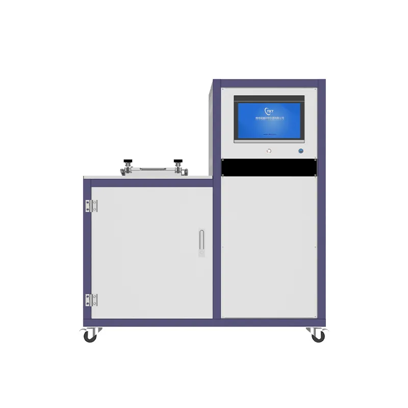
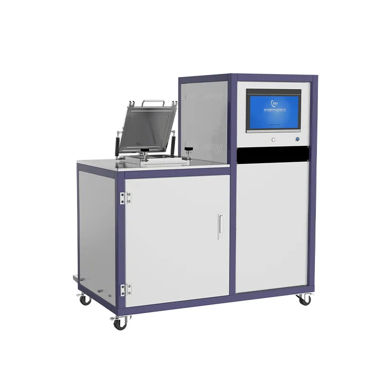
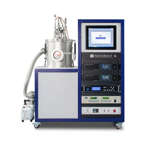
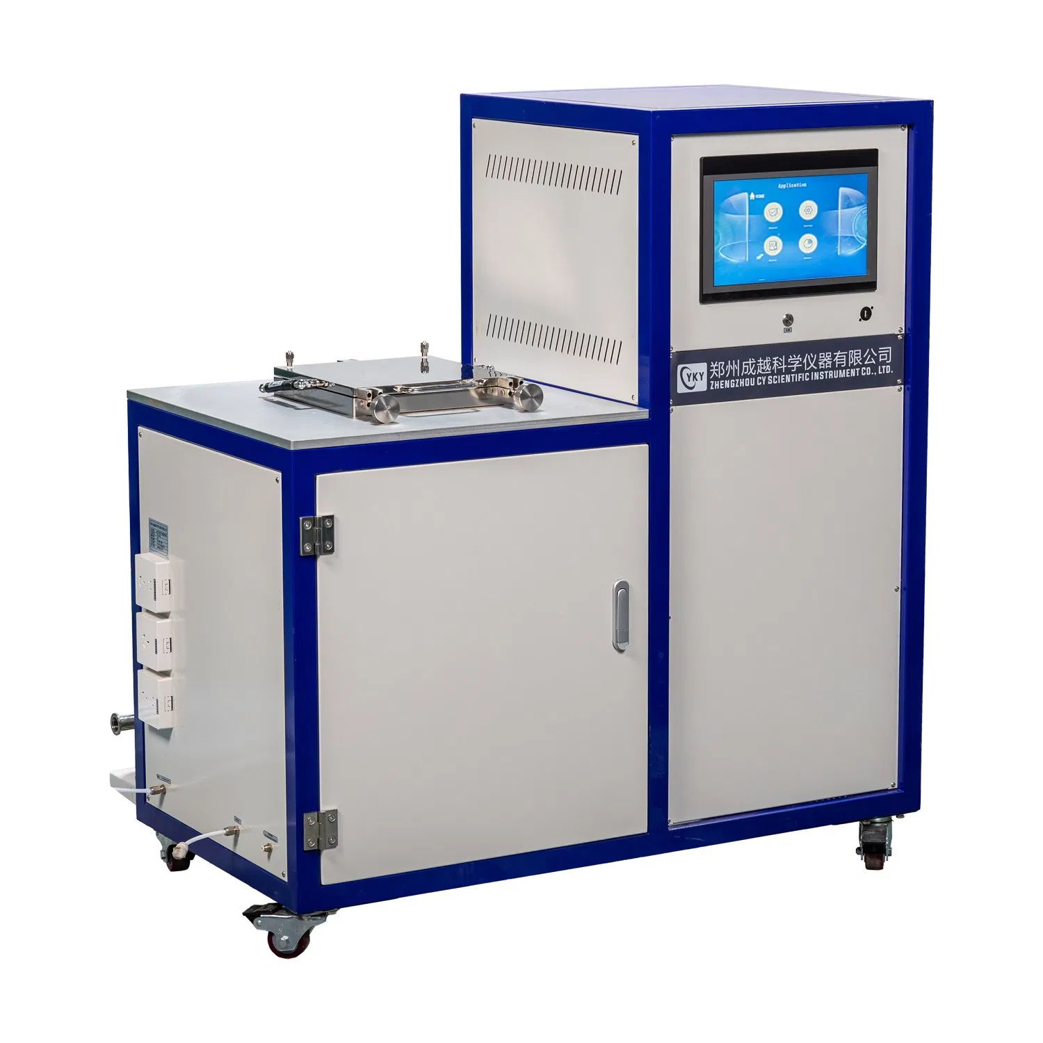
The Thermal Atomic Layer Deposition System is a specialized single-wafer deposition system designed for advanced scientific research and industrial pilot experiments. Fully compliant with CE criteria, it is widely utilized in micro-electronics, nano-materials, optical films, and solar battery technology.

Core Benefits
  • Advanced software control
  • Technological formulation integration
  • Precise parameter setting
  • Interlocking alarming system
  • Real-time state supervisory control
Supported ALD Films

Elementary: Co, Cu, Ta, Ti, W, Ge, Pt, Ru, Ni, Fe...
Nitride: TiN, SiN, AlN, TaN, ZrN, HfN, WN...
Oxide: TiO2, HfO2, SiO2, ZnO, ZrO2, Al2O3, La2O3, SnO2...
Others: GaAs, AlP, InP, GaP, InAs, LaHfxOy, SrTiO3, SrTaO6...
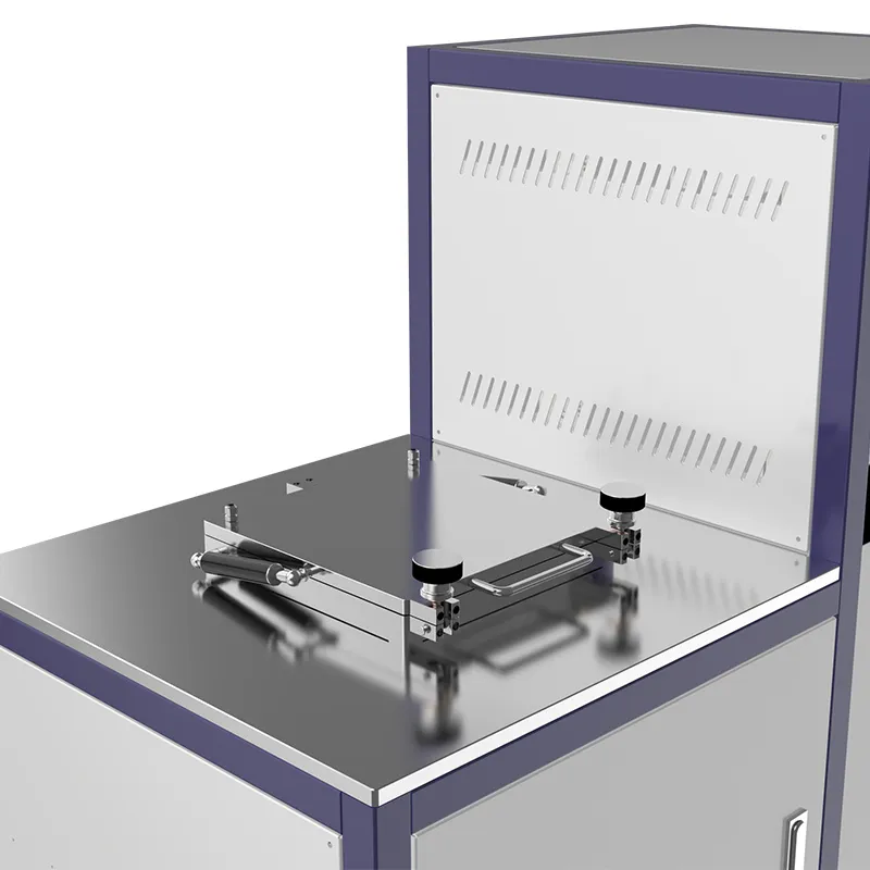
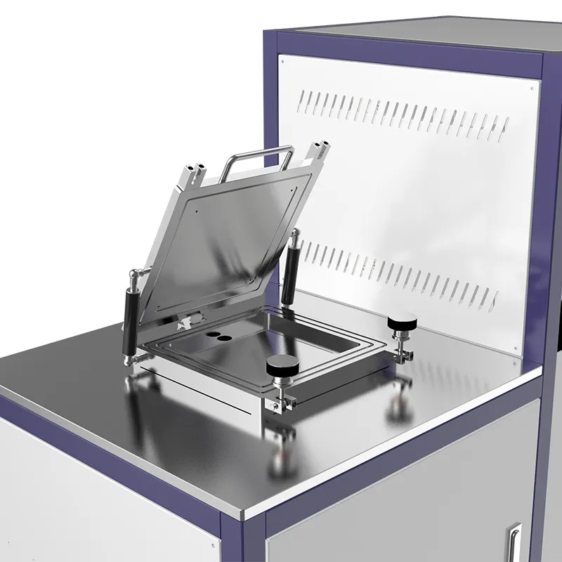
Application Fields
📍 High-k gate oxides
📍 Storage capacitor dielectrics
📍 Cu interconnect barriers
📍 OLED passivation layers
📍 MEMS coatings
📍 Solar battery cells
📍 Optical thin-films
📍 Nanoporous structures
Technical Parameters
Wafer Dimension8 inch and below
Wafer TemperatureRT-400ºC, Precision ±0.1ºC
Number of PrecursorThree precursor lines (optional more)
Precursor Line TempRT-200ºC, Precision ±0.1ºC
Source Bottle TempRT-200ºC, Precision ±0.1ºC
Background Vacuum<5*10-3 Torr
Growing ModeConsecutive or interval deposition
Power Supply50-60Hz, 220V/20A AC
Heterogeneity<±1%
Instrument Dimension600mm x 600mm x 1100mm
Detailed Photos
Technical Schematic
Frequently Asked Questions
Q: What is the main application of this ALD system?
A: It is primarily used for depositing high-k gate oxides, storage capacitor dielectrics, and pinhole-free passivation layers for OLEDs, MEMS, and solar cells.
Q: Can the system be customized for more precursor lines?
A: Yes, the standard configuration includes three precursor lines, but optional additional lines can be added based on specific research needs.
Q: What is the temperature control precision for wafers?
A: The system provides high-precision control within ±0.1ºC for wafer temperatures ranging from RT up to 400ºC.
Q: Does the equipment meet international safety standards?
A: Yes, the electric system of the ALD equipment completely accords with CE criteria, ensuring safety for laboratory and industrial use.
Q: How is the product protected during shipping?
A: All units are packaged in standard export fumigation-free wooden boxes to ensure safety during express, air, or sea transport.
Q: What type of after-sales support is provided?
A: We offer a 12-month warranty period with lifetime maintenance support and technical response within 24 hours.

Related Products